Last updated: February 1st, 2003
(First uploaded: April 10th, 2002)
|
(Two 8-bit I/O channels)
Contents of this document This document describes only the ISA card itself, not the additional components used for voltage, current, and temperature measuring. But for the sake of completeness I will mention that we've had great success using the MAX144 12 bit serial (SPI) A/D converters, the MAX472 bidirectional current sense amplifiers, both from Maxim, and the LM19 temperature sensor from National Semiconductors, all of which happen to be available as free samples. There is, of course, no reason not to use similar components from other vendors as well.
The ISA Bus One drawback of using the ISA bus is that it tends to be removed from current PCs and it might therefore become difficult to find a suitable computer in a couple of years. Unfortunately it isn't that easy to design a PCI or PCMCIA/PC-card solution. I'd love to have the same functionallity in a PC-card, though. You can find some fine documents descriping the ISA bus at www.epanorama.net. The most important stuff we'll have to know is this: The layout of the bus, the fact that only the lower 11 address bits are decoded by ISA cards, and that the timing isn't standardized.
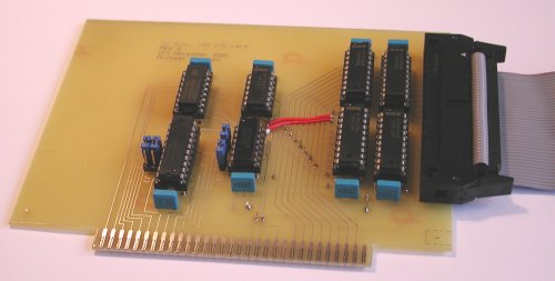
Address Decoding The address decoding is handled by a 74138 and a 74520. The 74520 compares address bit 3 to 10 (only the lower 11 bits of the 16 bit address bus is being decoded by ISA cards) to the value programmed by wires and two jumpers. The latter allows the user to select one of 4 base addresses, namely 300h, 310h, 320h, or 330h. None of these are used in most computers. This prevents resource conflicts with other parts of the computer, and allows several cards to be used in the same computer using different addresses on each card. The 138 receives the equal signal from the 520 and decodes the lower 3 bits into local chip select signals on the board. Two of these are combined with the io-read and io-write signals from the ISA bus and are used to generate output enable and latch enable signals for our 74574 registers. This allows the computer to read and write the registers on the board. In order for the external components to write into the registers we need them to set the latch enable signal. Since exact timing of this kind of event might not be needed, and since it, most likely, requires additional logic on the external part I decided to use two extra chip select signals from the 138 to enable the external latch enable signals. Therefore you can store input values in the registers by addressing (read or write) the register address + 4:
Two jumpers select whether you use internal or external latching. You need to close the jumpers for internal latching (described above), and you need to add two extra wires from U5, pin 2 to JP3 pin 18, and from U5, pin 5 to JP3 pin 24 in order to be able to use the external latching.
Timing One clock cycle is 1/16 Mhz = 62,5 ns. We have 5 levels of logic, each level is thus allowed 12,5 ns, which is fulfilled by both 74Fxx and 74ATCxx chips. You can consequently choose whatever is at hand - or cheaper.
Circuit Diagrams
I was going to upload a postscript version too, but it never turned out right, and to avoid scaling problems while printing I decided not to do it, so please use Protel if you want to print the pcb layout.
IMPORTANT |